Citing increased demand for its electronics application co-development expertise, Henkel today announced it has doubled the size of its Silicon Valley Application Center, relocating to a new site in Santa Clara, CA.
Jul 31, 2026 Irvine, CA
Henkel marks Silicon Valley Application Center growth with move to larger site with expanded technology
Commenting on Henkel’s investment in the recently opened facility and its strategic location, Kevin Becker, Senior Vice President of Product Development and Engineering for Electronics, notes the company’s dedication to supporting and partnering with customers in their local environments. “In recent years, Henkel has established or expanded several technical application centers in key locales around the world, including India, China, Singapore, and Vietnam, where side-by-side collaboration with our electronics and industrial customers helps expedite new product introduction for a competitive time-to-market advantage. Our Silicon Valley Application Center’s achievements to date and required expansion validate this approach and underscore Henkel’s ongoing commitment to customers and the communities where we live and work.”
The 15,000 sq. ft. Application Center, located in tech-centric Northern California, is home to a team of expert personnel who manage proof-of-concept consumer electronics work using state-of-the-art production, testing, and analytical systems. In addition to existing equipment, the new Henkel facility has expanded its technical team to continue its successful track record and product commercialization confidence. Henkel materials, including underfills, structural adhesives, encapsulants, and thermal control solutions, are significant determinants of electronic system functionality and reliability; evaluating their performance in application is essential.
Since establishing its Silicon Valley facility in 2022, Henkel and its customers have demonstrated what strong alliances, and real-time application validation can produce. The projects undertaken at the Henkel Application Center have led to advances in several cutting-edge consumer electronics applications, including systems powering data center AI and high-performance computing capability, as well as the latest consumer devices, such as XR/VR headsets and glasses.
“Demand for Henkel expertise has been continuously growing, shares Burcak Conley, Henkel Head of Application Engineering for Electronics for North America and Europe, saying, “Just four years after opening this site, we have already outgrown the space. From its inception, it was clear that this facility would be instrumental in supporting our customers’ innovation roadmaps, and we are thrilled that our collaborative work has necessitated additional resources. This milestone demonstrates Henkel’s commitment to fostering long-term partnerships, driving innovation, and creating value for our customers.”
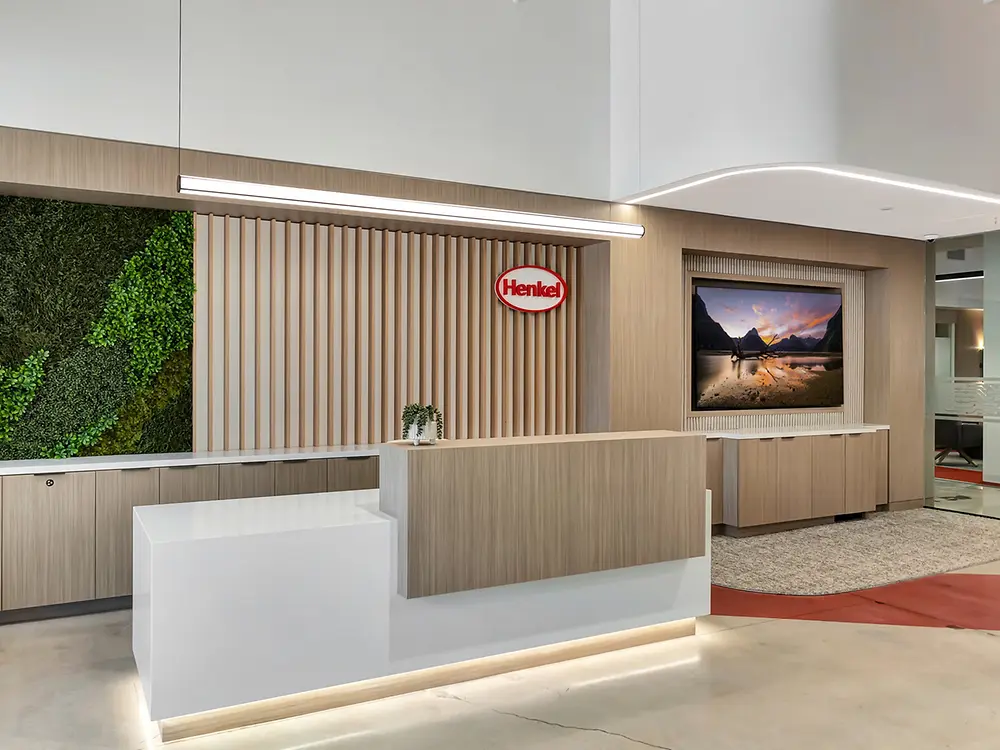
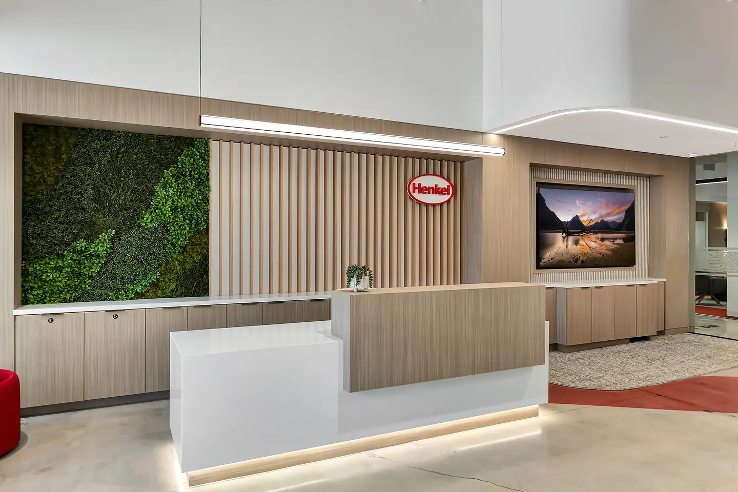
Henkel has opened its new Application Center for Electronics in Santa Clara, CA.
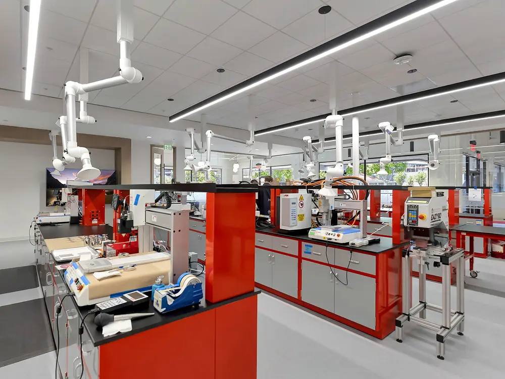

The new facility aims to strengthen regional customer collaboration and to accelerate new product development.
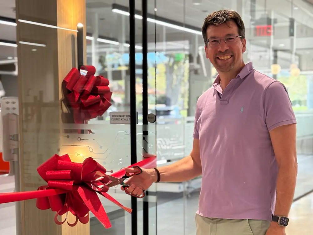

Mark Dorn, Executive Vice President for Henkel’s Adhesive Technologies business, joined the opening ceremony.
1 of 3